1. The Problem: Thickness Measurement Is Harder Than It Looks
In industries such as semiconductors, coatings, films, and batteries, thickness is everything. However, measuring it accurately is not straightforward as contact methods risk damage or contamination, and if laser or point sensors are used, they often struggle with transparent or multi-layer materials. Additionally, conventional vision systems cannot “see” thickness and are mainly suitable for surface inspection.
This becomes critical when the coatings are micron-level thin, materials are transparent or semi-transparent, or layers have similar visual appearance, resulting in hidden defects, inconsistent quality, and yield loss.
2. The Insight: Thickness Affects Light — Not Just Appearance
Thickness isn’t directly visible but it changes how light interacts with the material, and this is where Hyperspectral Imaging comes in.
Unlike standard cameras which utilizes RGB vision of 3 data points (Red, Green, Blue), hyperspectral contains hundreds of wavelengths per pixel, consisting a spectral signature, which reveals information such as absorption characteristics, reflectance variations, interference patterns. These spectral changes are directly correlated to material composition and layer thickness.
3. How It Works
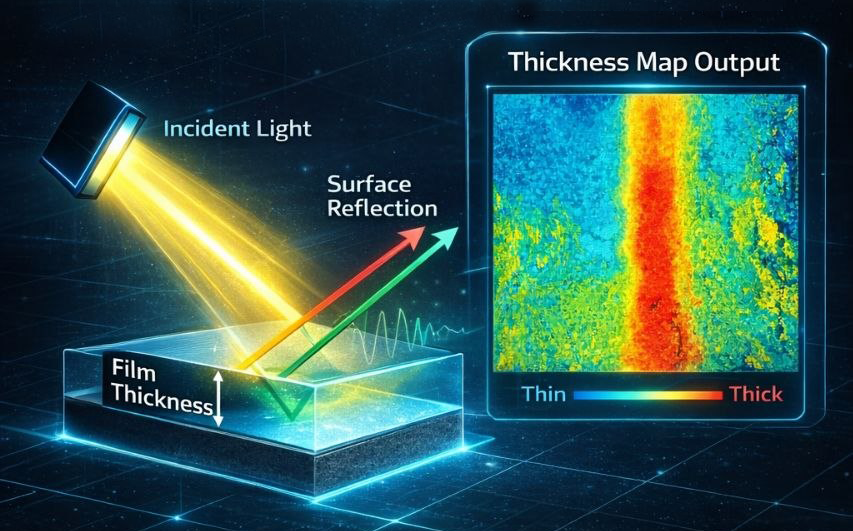
A broadband or controlled light source illuminates the sample and the hyperspectral camera captures reflected/transmitted light.
Each pixel produces a spectrum (not just intensity) and algorithms map spectral data whcih reveals the thickness values.
For thin films, light reflects from multiple interfaces and when Interference occurs, the resulting spectrum encodes thickness information.
4. The Solution: Non-Contact, High-Precision Thickness Measurement
Hyperspectral imaging enables:
Non-contact measurement
No risk of damaging delicate surfaces
Works on transparent & multi-layer materials
Glass, films, coatings, polymers
Full-field inspection (not just a point)
Detect local variations, not just averages
Inline capability
Especially powerful with line-scan systems
5. Where It Delivers the Most Value
Semiconductor & Electronics
- Photoresist thickness
- Wafer coatings
- Thin film uniformity
Battery Manufacturing
- Electrode coating thickness
- Uniformity across large areas
Optical Films & Displays
- Polarizers, OLED layers
- Functional coatings
Industrial Coatings
- Paint, adhesives, protective layers
6. Why Lighting Matters (Critical but Often Overlooked)
For hyperspectral thickness measurement, lighting is not just illumination — it’s data quality.
Key considerations:
- Spectral stability → consistent measurements
- High brightness → better signal-to-noise
- Uniformity → accurate mapping across FOV
- Wavelength selection → sensitivity to thickness range
This is where advanced illumination (e.g. broadband, SWIR, or tunable sources) becomes critical.
7. Key Takeaway
Thickness may be invisible to the eye but it is highly visible in the spectral domain.
Hyperspectral imaging transforms thickness measurement from indirect, contact-based, limited to non-contact, data-rich and scalable.